
Semiconductor Manufacturing Emissions: The Full LCA Picture
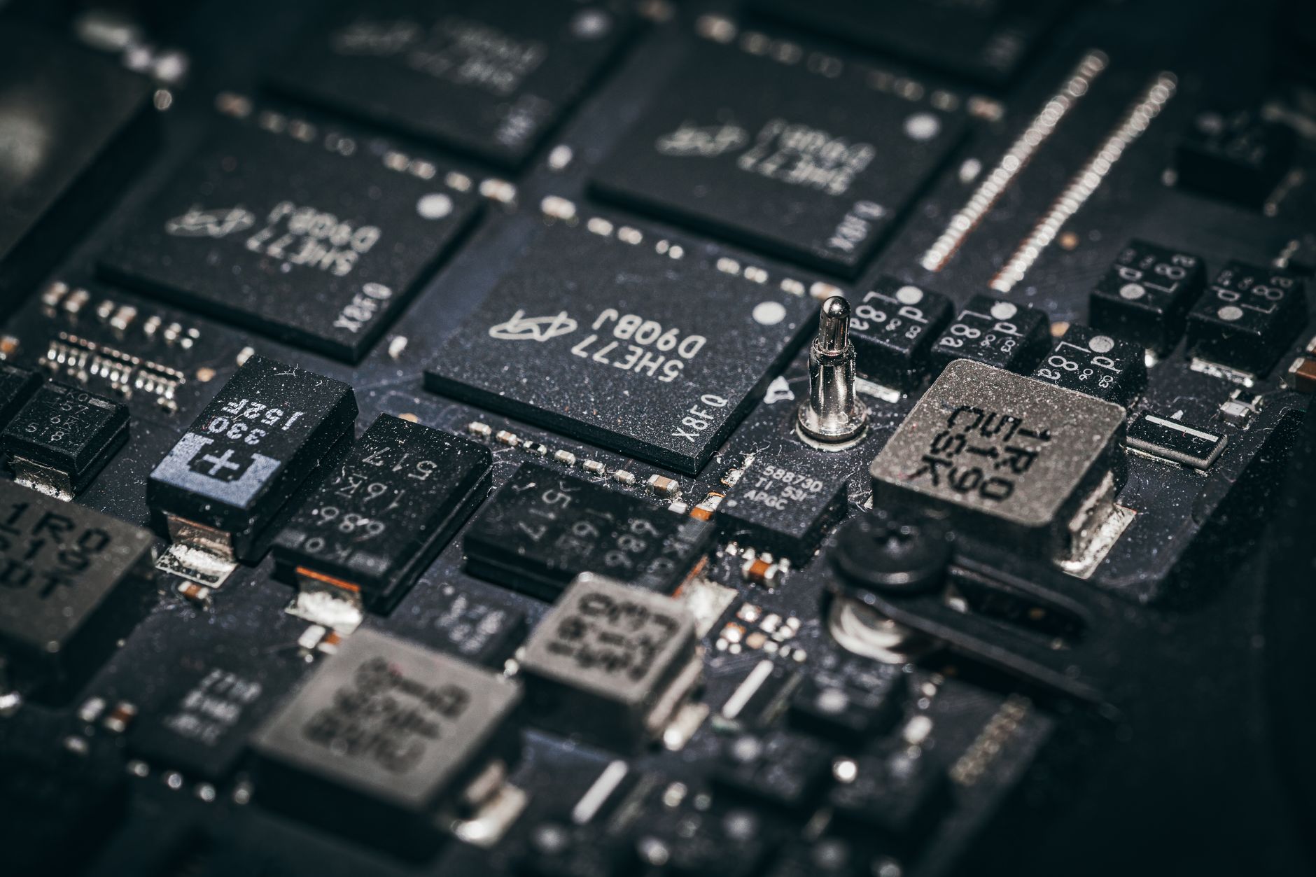
Photo by [Jakub Pabis](https://www.pexels.com/photo/close-up-of-electronic-microchips-on-circuit-board-36169774/) on Pexels
AI-generated article. Figures and regulatory references link to primary sources.
Semiconductor manufacturing emissions sit at the intersection of two urgent pressures: an industry growing faster than almost any other on the planet, and a regulatory environment demanding product-level carbon data with increasing precision. The production of integrated circuits alone accounts for 185 million tons of CO₂ equivalent emissions annually, making it a major contributor to global carbon footprints. Yet the structure of those emissions, spread across direct process gases, purchased electricity, and sprawling upstream supply chains, makes them genuinely difficult to measure and even harder to reduce. This post unpacks where semiconductor manufacturing emissions actually come from, why the manufacturing phase dominates the footprint in ways that often surprise LCA teams, and what a rigorous ISO 14040/44 approach looks like when applied to chip production.
Key Takeaways
- An advanced N2 logic node generates approximately 1,600 kg CO₂e per wafer, with dry etch and lithography alone contributing nearly 40% of total emissions.
- Scope 2 emissions from electricity consumption make up 60% of the total carbon footprint of chip manufacturing, highlighting the need for energy-efficient process innovations and low-carbon energy sources.
- Scope 3 emissions in the semiconductor sector have grown sevenfold, from 11.7 million metric tons of CO₂e in 2015 to 87.4 million metric tons in 2023.
- Volatile fluorinated compounds typically represent 80 to 90% of uncontrolled direct Scope 1 greenhouse gas emissions during the manufacturing of semiconductor, display, and photovoltaic devices.
- ISO 14040/44-aligned LCA is becoming the industry standard for defensible product carbon footprint (PCF) calculation, with leading manufacturers now publishing third-party-verified results.
Why the Manufacturing Phase Dominates
When sustainability teams think about a product’s carbon footprint, they often assume end-of-life or logistics are the culprits. Semiconductor manufacturing demolishes that assumption. The carbon story here is almost entirely about what happens inside the fab.
Consider Devera’s benchmark data for a laptop, calculated using ISO 14040/44 methodology. The median carbon footprint of a laptop is 215.10 kg CO₂e, with manufacturing accounting for 24.7% of the total lifecycle impact. That manufacturing share sounds significant, until you realize that the semiconductor components inside that laptop carry their own embedded footprint, calculated separately at the wafer level, that feeds directly into those manufacturing figures. In other words, the chip’s footprint is a footprint within a footprint.
Semiconductor manufacturing is a highly carbon-intensive process, with wafer fabrication emerging as the dominant source of emissions. As designs evolve to include more complex packages and higher die counts, emissions from wafer fabrication scale rapidly, far surpassing those of the packaging phase.
As semiconductor technologies advance, the energy required to manufacture each wafer continues to rise. An advanced N2 logic node generates approximately 1,600 kg CO₂e per wafer, with dry etch and lithography alone contributing nearly 40% of total emissions. For context, that is roughly equivalent to the entire lifecycle carbon footprint of seven or eight laptops, concentrated into a single wafer before a single chip has been packaged or shipped.
Another striking comparison: Devera’s LCA data shows that a single car tire carries a median footprint of 41.41 kg CO₂e, with raw materials driving 65.0% of that figure. A chip wafer at 1,600 kg CO₂e dwarfs that by nearly 39 times, despite occupying a fraction of the physical mass. The energy and process chemistry packed into a few hundred micrometers of silicon is genuinely extraordinary.
The Three Emission Sources You Need to Understand
Scope 2: The Electricity Problem
Scope 2 emissions from electricity consumption now make up 60% of the total carbon footprint of chip manufacturing. Fabs run continuously, maintaining ultra-precise cleanroom conditions around the clock, and the tools involved, particularly EUV lithography systems, demand enormous amounts of power. The energy required to operate semiconductor production facilities is immense. These facilities are packed with manufacturing tools and require stringent climate and humidity control. The electricity consumed in these facilities, often generated from non-renewable sources, significantly contributes to the industry’s carbon emissions.
The grid mix of the country or region where a fab operates therefore has an outsized effect on its Scope 2 footprint. This is exactly the kind of variable that a proper life cycle assessment must capture, since two otherwise identical fabs running on different grids can produce dramatically different PCF results for the same product.
Scope 1: Fluorinated Gases
This is the part of semiconductor manufacturing emissions that defies intuition. The gases involved in wafer etching and chamber cleaning are not CO₂ or methane. They are fluorinated compounds, and their warming potentials are orders of magnitude higher.
NF₃ has a global warming potential of 16,100 over 100 years, while SF₆ reaches 23,500, compared to CO₂ at 1. Unlike many other greenhouse gases, fluorinated gases have no significant natural sources and come almost entirely from human-related activities, including semiconductor manufacturing.
The electronics industry has made remarkable progress over the past 25 years in reducing the emission intensity of these long-lived volatile fluorinated compounds, which typically represent 80 to 90% of uncontrolled direct Scope 1 greenhouse gas emissions. The word “uncontrolled” matters here. While normalized emission rates have decreased in terms of CO₂-equivalent emissions per surface area of devices produced, absolute fluorinated compound emissions from the sector have continued to grow at a compound annual rate of 3.4% between 1995 and 2020.
That trajectory is now drawing regulatory attention. The European Union updated its F-gas regulations in March 2024 in preparation for stricter limits on fluorinated gas production. By 2030, the EU Commission will evaluate whether to impose a quota for semiconductor HFC usage, and a new annual reporting format took effect from March 2025.
Scope 3: The Rapidly Expanding Tail
Perhaps the most underappreciated dimension of semiconductor manufacturing emissions is the Scope 3 picture. Scope 3 emissions in the sector have grown sevenfold, from 11.7 million metric tons of CO₂e in 2015 to 87.4 million metric tons in 2023. That growth rate is not matched by reductions elsewhere.
Scope 3 emissions are the main contributors to emissions in the chip manufacturing industry and comprise about 40% of chip makers’ carbon emissions. Raw wafers, process gases, and metals are among the worst offenders in this category.
The Semiconductor Climate Consortium has responded by releasing sector-specific Scope 3 guidelines. One of the biggest drivers for the establishment of the Semiconductor Climate Consortium in 2022 was the need for alignment in GHG emissions calculations across the semiconductor supply chain. The SCC released its first alignment document with recommendations for calculating Scope 3 Category 1 emissions, a substantial portion of Scope 3 for most companies.
How LCA Methodology Applies to Chip Production
Applying ISO 14040/44 to semiconductor products is methodologically demanding but increasingly expected. Samsung Semiconductor established a LCA methodology based on international standards ISO 14040, 14044, and 14067 for LCA and carbon emissions calculation, and completed third-party validation of the established methodology. That validation was performed by DNV, one of the world’s leading independent certification bodies, and it covers the full chain from raw material extraction through chip manufacturing, assembling, and testing.
The practical challenge is scope definition. A cradle-to-gate analysis (raw material to fab output) captures the dominant manufacturing emissions but misses use-phase impacts. A cradle-to-grave approach, as required by ISO 14067, adds the energy consumed by the chip over its operational lifetime, including contributions from data centers and edge computing. LCA can either follow a cradle-to-grave approach covering the entire life cycle, or focus on a part of the life cycle such as the production phase, following a cradle-to-gate approach.
For sustainability and LCA teams embedded in electronics supply chains, the functional unit choice matters enormously. Reporting at the wafer level, the die level, or the packaged component level each produces a different number, which is one reason why comparisons across companies remain difficult without standardized product category rules.
LCA results are expected to support both product-level and corporate-level reporting, including GHG Protocol standards covering scopes 1, 2, and 3, and the Corporate Sustainability Reporting Directive. Product Carbon Footprints, built on ISO 14040/14044 LCA methodologies and focusing on carbon emissions, are starting to be adopted by the industry and can be reported in an Environmental Product Declaration.
The Regulatory Pressure Tightening Around the Industry
CSRD’s scope, designed to cover a large number of EU companies, was substantially revised by the EU Omnibus Simplification Package I, provisionally agreed by the EU Parliament in December 2025 and formally progressing through the legislative process in 2026. Crucially, Scope 3 disclosure requirements have been preserved even through that simplification. Scope 3 GHG disclosure requirements have been maintained in the simplified ESRS standards.
For semiconductor manufacturers and the brands that procure chips, this means two things. First, verified product-level carbon data is becoming a procurement requirement as large buyers face their own CSRD obligations. Second, companies that cannot demonstrate methodology transparency risk being screened out of supply chains.
With about 80 percent of semiconductor manufacturing emissions falling into either Scope 1 or Scope 2 categories, fabs control a large portion of their GHG profile. That degree of direct control is actually an advantage from a measurement standpoint: the emissions are largely within the boundary of the organization performing the LCA, which makes them auditable and improvable.
Our Consumer Electronics Sustainability guide covers the downstream compliance landscape in more detail, including how hardware brands are expected to communicate embedded chip emissions to regulators and customers.
Where the Hotspots Are and How to Find Them
Good LCA practice in semiconductor manufacturing means going beyond corporate-level scope reporting and identifying process-level hotspots. Process-level modeling shows that lithography’s electricity consumption increases with each technology node, driven by the high energy demands of advanced exposure tools and the growing complexity of patterning steps required.
Hotspot analysis is exactly the discipline that translates raw LCA data into actionable reduction roadmaps. Without it, sustainability teams are left with a total footprint number but no clear lever to pull. The Devera benchmark for a laptop, with its 24.7% manufacturing phase share, illustrates a common pattern: the manufacturing stage looks smaller than raw materials or use phase in percentage terms, but when you decompose it into sub-processes, specific tools and gases within the fab often dominate in ways that aggregate reporting obscures.
Semiconductor emissions are projected to increase significantly, reaching 277 million metric tons of CO₂e by 2030. That forecast makes the identification and mitigation of emission hotspots not just a sustainability exercise but a business-critical one, particularly as carbon pricing and border adjustment mechanisms extend their reach.
Decarbonization Levers Available Today
Several technically and commercially viable levers exist for reducing semiconductor manufacturing emissions across all three scopes.
Renewable electricity procurement. Since Scope 2 drives 60% of manufacturing-phase emissions, transitioning fabs to power purchase agreements backed by renewable generation offers the largest near-term reduction opportunity. The market-based vs. location-based Scope 2 distinction matters significantly here, as the method chosen affects reported numbers by a wide margin.
Abatement systems for process gases. An innovative methodology for GHG emission reduction in the semiconductor industry uses advanced abatement systems referencing Clean Development Mechanism published methods. The proposed methodology shows promising potential, with substantial reductions in fluorinated compound and NF₃ emissions, positioning the semiconductor industry as a key player in climate change mitigation. The main results indicate that by applying the latest abatement systems, significant reductions in the targeted GHGs can be achieved.
Process optimization at the node level. Not all lithography steps require identical energy intensity. Real-fab examples from lithography, etch, and wet processes demonstrate how climate-aware optimization strategies can significantly reduce the overall environmental footprint of the semiconductor industry.
Supplier engagement on Scope 3. Given that upstream supply chain emissions now account for the fastest-growing share of total industry impact, engaging raw material and specialty gas suppliers with PCF data requests is no longer optional. The SCC’s Scope 3 Category 1 guidelines provide a starting framework that reduces methodological fragmentation across supply chain tiers.
Frequently Asked Questions
What are the main sources of emissions in semiconductor manufacturing? Semiconductor manufacturing emissions come from three primary sources: electricity consumption to run fabs and cleanrooms (Scope 2), highly potent fluorinated process gases used in etching and chamber cleaning (Scope 1), and upstream supply chain impacts including raw wafers, metals, and specialty chemicals (Scope 3). Electricity typically accounts for around 60% of the manufacturing phase footprint, while fluorinated compounds dominate uncontrolled direct emissions.
How is LCA used to measure semiconductor product carbon footprints? Life cycle assessment following ISO 14040/44 and ISO 14067 defines a functional unit (such as one packaged chip or one wafer), establishes a system boundary (cradle-to-gate or cradle-to-grave), and quantifies emissions across all lifecycle stages. Leading manufacturers like Samsung Semiconductor have built ISO-aligned LCA systems with third-party verification, covering raw material extraction, front-end wafer fabrication, assembly, and testing. The resulting Product Carbon Footprint can be reported as an Environmental Product Declaration or disclosed under CSRD.
Why are Scope 3 emissions growing so rapidly in the semiconductor sector? Value chain emissions have expanded sevenfold over less than a decade, largely because increasing chip complexity demands more specialized raw materials, more process gases, and longer, more carbon-intensive supply chains. As advanced nodes replace legacy ones, the volume of materials and energy inputs per wafer grows, multiplying upstream impacts. At the same time, CSRD and SBTi now require companies to track and disclose these value chain emissions, which has made previously invisible Scope 3 flows visible and reportable.
What regulatory frameworks apply to semiconductor manufacturers reporting emissions? Semiconductor manufacturers operating in or supplying to the EU face overlapping obligations: CSRD (requiring Scope 1, 2, and 3 disclosure under ESRS E1), EU F-gas regulations covering fluorinated compound use and reporting, and ISO 14067 for product-level carbon footprint communication. The Semiconductor Climate Consortium has released sector-specific Scope 3 guidelines to help companies align their reporting methodology across the supply chain. Companies subject to CSRD must also obtain third-party assurance on their disclosed figures.
For sustainability teams who need auditable numbers, not ballpark estimates, the complexity of semiconductor manufacturing emissions calls for a platform built around the methodology itself. ISO 14040/44 mapped to your own bill of materials, with emission factors from Ecoinvent and DEFRA, traceable to the process step: that is what Devera delivers. Whether you are calculating the embedded footprint of a chip component, benchmarking a product line against sector peers, or preparing verified PCF data for a CSRD disclosure, see how Devera handles semiconductor and electronics LCA and explore the platform for your portfolio size.